Overview
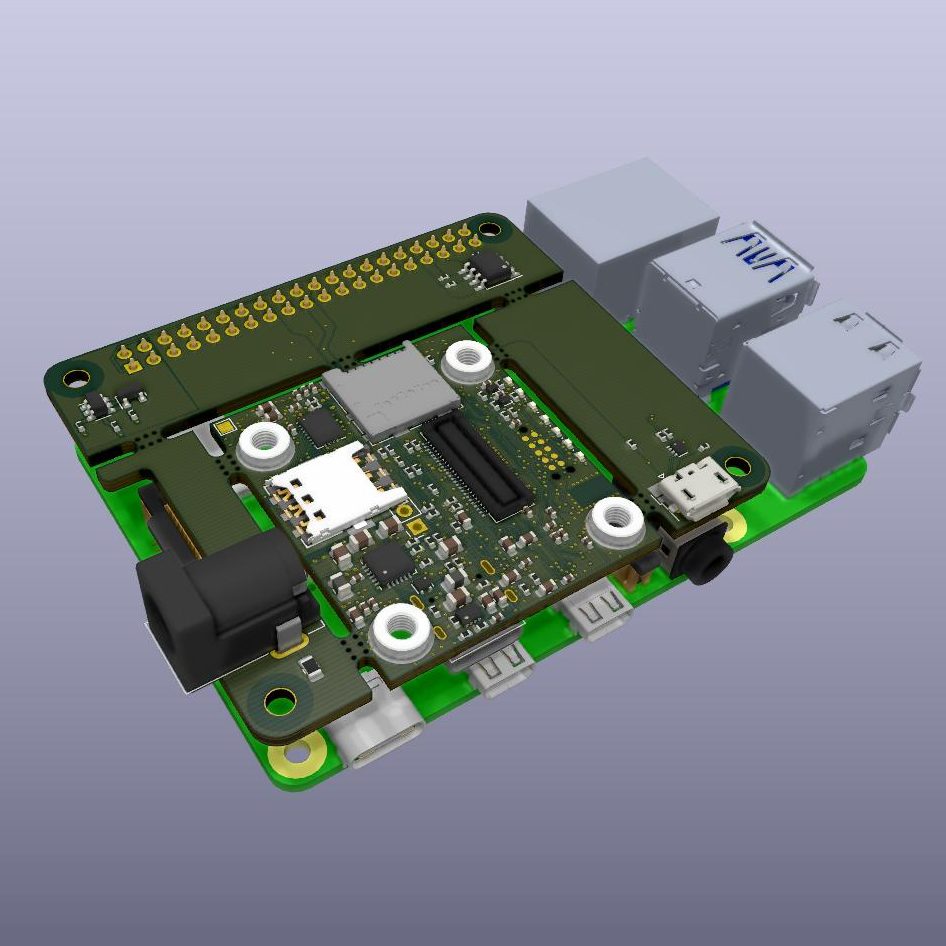
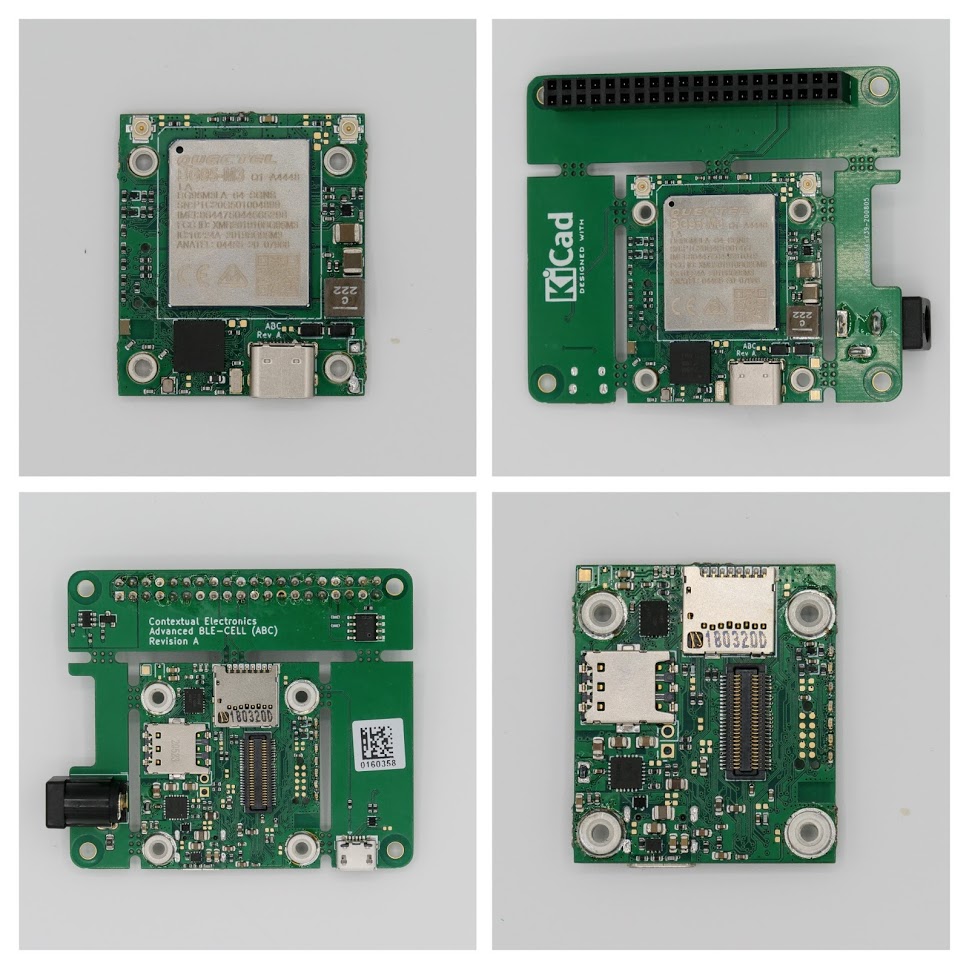
This is a course focused on building out a Raspberry Pi HAT with Bluetooth and Cellular on it. This board has 3 intended purpose at creation:
- Education for CE Members
- Development platform for easy access to a cellular and bluetooth design
- Reference design for future build outs, including other Zephyr based systems
Prerequisites
- None
This course in the style of an “Apprenticeship”, where the viewer is not expected to have all required elements, but will still be able to learn from watching the design process and layout of a board.
Learning Objectives
- High complexity routing of a 4 layer PCB
- Creating a platform, as opposed to a one-off board
- Understand the interaction between high complexity components, such as a bluetooth SOC and a cellular SOM
- Use the open source Zephyr RTOS to create an extensible firmware/software ecosystem
- Create “daughtercards” to create additional functionality using sensors and other components
Future Plans
This board will be offered for sale by Q2 of 2021. This will allow members to use this design for their own projects, or to create add-on boards for rapid prototyping.
Documentation
The ABC board and daughterboards are not currently licensed as OSHW, but schematic(s) is available below
Access
This is a paid course, available to Apprentice, Journeyman, and Master Members of Contextual Electronics. Select course modules are available without a subscription, notably the top level “Lessons”.


A public overview video, recorded 11/16/20
Course Content
Design Planning
-
Starting the KiCad project and importing components
-
Adding the ABC project to Github
-
Adding the BG96 to the ABC
-
Incoming power system and battery setup
-
Looking at standoffs and the Z height between snap-off PCBs
-
Revising the block diagram to match the layout and reconsidering power domains
-
Re-drawing the ABC board outline to include the edge cuts and the slot for the camera
-
Adding the RPi 3D model as a reference point and placeholder
-
ABC Blocks and Budget
-
Daughtercard connector and SIM card holder height
-
Pulling In Battery and USB connector 3D models
-
Final mechanical refactor of the ABC before moving onto electrical design
- Starting the KiCad project and importing components
- Adding the ABC project to Github
- Adding the BG96 to the ABC
- Incoming power system and battery setup
- Looking at standoffs and the Z height between snap-off PCBs
- Revising the block diagram to match the layout and reconsidering power domains
- Re-drawing the ABC board outline to include the edge cuts and the slot for the camera
- Adding the RPi 3D model as a reference point and placeholder
- ABC Blocks and Budget
- Daughtercard connector and SIM card holder height
- Pulling In Battery and USB connector 3D models
- Final mechanical refactor of the ABC before moving onto electrical design
Choosing components and doing preliminary placement
-
Implementing a simple 3V3 Buck Regulator
-
Searching for the 3V8 Regulator
-
Reviewing Block Diagram Inputs To 3V8 Regulator
-
Comparing TI Battery Management ICs
-
Choosing the battery management IC and looking at extra features
-
Roughing in the battery management solution
-
Finding the battery management inductor
-
Pulling in the SIM card holder and daughtercard connector
-
Battery management schematic cleanup and board reorg
-
Adding a logic level translator and JTAG header
-
Modifying uFL positions and adding 2.4GHz chip antenna
-
Simplifying the main board block diagram
-
Flipping the script (components)
-
Adding a serial switch (mux) for changing control between the BLE and CELL modules
-
Switching to a 50 pin daughtercard header
-
Simplifying UART comms and adding a new interface to the modem
-
BOM cleanup and price estimation
-
Adding support components to the schematic for the nRF52
-
Adding support components for the BG95/EG91
-
Cleanup of power input
-
Cleanup of connections
- Implementing a simple 3V3 Buck Regulator
- Searching for the 3V8 Regulator
- Reviewing Block Diagram Inputs To 3V8 Regulator
- Comparing TI Battery Management ICs
- Choosing the battery management IC and looking at extra features
- Roughing in the battery management solution
- Finding the battery management inductor
- Pulling in the SIM card holder and daughtercard connector
- Battery management schematic cleanup and board reorg
- Adding a logic level translator and JTAG header
- Modifying uFL positions and adding 2.4GHz chip antenna
- Simplifying the main board block diagram
- Flipping the script (components)
- Adding a serial switch (mux) for changing control between the BLE and CELL modules
- Switching to a 50 pin daughtercard header
- Simplifying UART comms and adding a new interface to the modem
- BOM cleanup and price estimation
- Adding support components to the schematic for the nRF52
- Adding support components for the BG95/EG91
- Cleanup of power input
- Cleanup of connections
ABC Layout
-
ERC Checking
-
nRF52 Support Component Placement
-
BG95-EG91 Support Component Placement
-
Battery management component placement
-
3V3 regulator component placement
-
Choosing a board house by spacing capabilities
-
Initial Power Plane Placement
-
Escaping the nRF52 pads on a 3.5 mil PCB process
-
More nRF52 breakout and connector layout
-
Initial power supply control signal layout
-
Finishing connecting power supply signals
-
The perils of inserting a forgotten component (TVS diodes)
-
Finishing connecting the nRF52
-
Routing level translator and SIM card components to BG95
-
Finishing connections to the BG95
-
Adding mousebites and cleaning up non-RF connections
-
Controlled impedance for RF traces on the ABC
-
Re-routing USB controlled impedance lines
-
Adding new breaktabs and OpenOCD capabilities
-
Adding the 2.4G antenna and clearance area
-
Reviewing RF changes and finalizing RF connections
-
Cleaning up all ABC DRC errors
-
Copper cleanup, adding silkscreen, and generating gerbers
-
Generating ABC output files and ordering PCBs
-
Revising design based on CAM feedback
-
A conversation with Roy Chen, Quectel FAE
-
Revising the design based on Quectel feedback
-
Final CAM fixes (with unknown problems)
-
Creating a fab drawing template using a footprint
- ERC Checking
- nRF52 Support Component Placement
- BG95-EG91 Support Component Placement
- Battery management component placement
- 3V3 regulator component placement
- Choosing a board house by spacing capabilities
- Initial Power Plane Placement
- Escaping the nRF52 pads on a 3.5 mil PCB process
- More nRF52 breakout and connector layout
- Initial power supply control signal layout
- Finishing connecting power supply signals
- The perils of inserting a forgotten component (TVS diodes)
- Finishing connecting the nRF52
- Routing level translator and SIM card components to BG95
- Finishing connections to the BG95
- Adding mousebites and cleaning up non-RF connections
- Controlled impedance for RF traces on the ABC
- Re-routing USB controlled impedance lines
- Adding new breaktabs and OpenOCD capabilities
- Adding the 2.4G antenna and clearance area
- Reviewing RF changes and finalizing RF connections
- Cleaning up all ABC DRC errors
- Copper cleanup, adding silkscreen, and generating gerbers
- Generating ABC output files and ordering PCBs
- Revising design based on CAM feedback
- A conversation with Roy Chen, Quectel FAE
- Revising the design based on Quectel feedback
- Final CAM fixes (with unknown problems)
- Creating a fab drawing template using a footprint
Hands-on with the ABC
-
Touring the new lab
-
ABC Initial Power Testing
-
ABC battery charge testing and troubleshooting
-
Getting to Blinky on the nRF52840-DK
-
Programmer options for the ABC
-
Connecting the JLink to the ABC
-
Setting up ABC pins for blinking LEDs
-
Getting to Blinky on the ABC using the nRF5 SDK
-
(Not) Getting to Bluetooth on the ABC (?)
-
Getting to Blinky with Zephyr on the nRF52840-DK
-
Getting to Blinky with Zephyr on the ABC board
-
Setting up Eclipse debugging with Bilal
-
Setting up PWM in Zephyr on the ABC
- Touring the new lab
- ABC Initial Power Testing
- ABC battery charge testing and troubleshooting
- Getting to Blinky on the nRF52840-DK
- Programmer options for the ABC
- Connecting the JLink to the ABC
- Setting up ABC pins for blinking LEDs
- Getting to Blinky on the ABC using the nRF5 SDK
- (Not) Getting to Bluetooth on the ABC (?)
- Getting to Blinky with Zephyr on the nRF52840-DK
- Getting to Blinky with Zephyr on the ABC board
- Setting up Eclipse debugging with Bilal
- Setting up PWM in Zephyr on the ABC
Creating a daughtercard (ABCDCBA)
-
ABCDCBA – Starting the template file
-
ABCDCBA – Doubling up the connectors
-
ABCDCBA – Swapping Bottom Connector to DP50 version
-
ABCDCBA- Adding Sensors Supported in Zephyr
-
ABCDCBA – Rethinking multiple connectors
-
ABCDCBA – Adding the remainder of schematic symbols
-
ABCDCBA – Adding footprints for remaining components
-
ABCDCBA – Checking ABC Clearances
-
ABCDBCA – Placement and Layout
-
ABCDCBA – Revising design for larger design features
-
ABCDCBA – Board review before assembly
- ABCDCBA – Starting the template file
- ABCDCBA – Doubling up the connectors
- ABCDCBA – Swapping Bottom Connector to DP50 version
- ABCDCBA- Adding Sensors Supported in Zephyr
- ABCDCBA – Rethinking multiple connectors
- ABCDCBA – Adding the remainder of schematic symbols
- ABCDCBA – Adding footprints for remaining components
- ABCDCBA – Checking ABC Clearances
- ABCDBCA – Placement and Layout
- ABCDCBA – Revising design for larger design features
- ABCDCBA – Board review before assembly