Summary
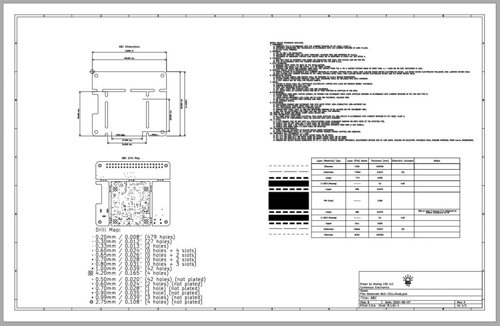
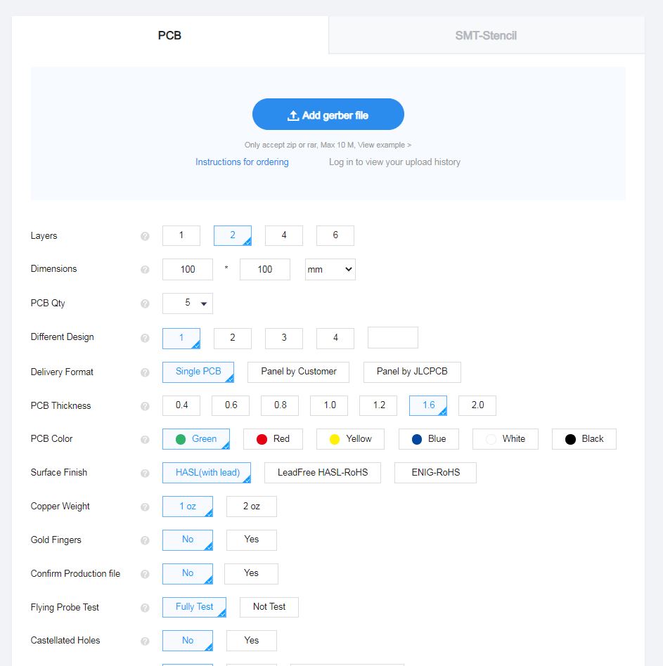
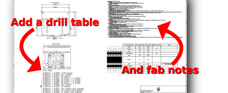
In the video below, we’re adding more information to our fabrication drawing for our PCB, including a drill table and fab notes. This allows us to get a board quoted or manufactured by a wider range of PCB houses than the online options. The online fab services capture all of this information in an online form dialog, like the one shown at the bottom of this post. Instead, we will add the required information to our fab drawing. With a fab drawing, we have a record of what we want the PCB to look like and what the critical specifications are.
Watch the associated video
This post is associated with a video on YouTube. Watch it below or over on YouTube.com.
Adding a drill table to your fab drawing
We use KiCad for all Contextual Electronics projects. If you use a different layout tool, you will need to figure out how to generate and add a drill table. The idea is the same for all designs though: we want to indicate how many different size drills are used on the PCB shown, and how many drill operations are required. This will impact the cost of the PCB because more drills means more time spent on the machines that do the drilling. See this time-tagged link to Scotty’s video tour of JLC (Strange Parts) to see how drilling is done.
KiCad has a tool buried in the “generate drill file” dialog. Normally this dialog is used to generate a .drl file, which gives all details about the location of drills and is used to actually program the machine that does the drilling. There is also a “generate map” button in the lower right, which will generate a vector based image showing where all of the various drill types are located on a particular PCB. After we generated this
Adding fab notes to your fab drawing
Fab notes are there to tell your manufacturer the detailed build information for creating your PCB. In an era before online tools (screenshot example below), this was the only way to get information across in a standardized manner. Many PCB fabs without an online interface requires fab drawings to ensure they are making a PCB that the engineer and company requesting the board actually wants. This includes details like the soldermask color, the silkscreen color, the overall board thickness, inspection requirements (IPC), or any other requests you have.
We recently were pointed at this article from Supplyframe Hardware about some standardized notes you can add to your drawing. This is not an exhaustive list, but it includes a good “starting point” for people that are new to building out their fab drawings for working with traditional PCB fabs. It’s also possible to include the fab drawing with your designs going to online PCB houses, to ensure they are hitting your requirements. Be sure to call out the fab drawing (and remember to upload it) when you are submitting your design.
Previous video about fab drawings
In the previous video about fab drawings (below), we discussed the stackup and how to create your own. We also linked to our library of templates for adding to your drawings.
Learn more about the ABC board
The ABC board shown in this video is part of a many part series (100+ videos) showing the entire design, board bringup, and firmware design of a cellular and bluetooth device. New members can try a week of Contextual Electronics for free.
Example PCB Fab Drawing

Click the image above for a PDF version of the fab drawing
Example online selection tool
This is a screenshot of a popular online PCB provider (JLC). Interfaces such as these allow for a standardized quoting process and fast-forwards board ordering, compared to how PCB orders traditionally are done. However, with these interfaces you have less overall control. You are basically ordering from a standard offering.

